Datasheet extraction, module specs, marketing photos, and
project CLAUDE.md with local resource inventory.
9.5 KiB
Document Metadata
Format: PDF 1.4 Title: HMC472A (v02.0420) Author: Analog Devices, Inc. Subject: 0.5 dB LSB GaAs MMIC 6-Bit Digital Positive Control Attenuator, DC - 3.8 GHz Creator: Adobe InDesign 14.0 (Windows) Producer: Adobe PDF Library 15.0 Creation Date: D:20200416094000-04'00' Mod Date: D:20200416094124-04'00'
Page 1
ATTENUATORS - DIGITAL - SMT 1 HMC472ALP4 / 472ALP4E v02.0420 0.5 dB LSB GaAs MMIC 6-BIT DIGITAL POSITIVE CONTROL ATTENUATOR, DC - 3.8 GHz For price, delivery, and to place orders: Analog Devices, Inc., One Technology Way, P.O. Box 9106, Norwood, MA 02062-9106 Phone: 781-329-4700 • Order online at www.analog.com Application Support: Phone: 1-800-ANALOG-D Information furnished by Analog Devices is believed to be accurate and reliable. However, no responsibility is assumed by Analog Devices for its use, nor for any infringements of patents or other rights of third parties that may result from its use. Specifications subject to change without notice. No license is granted by implication or otherwise under any patent or patent rights of Analog Devices. Trademarks and registered trademarks are the property of their respective owners. Functional Diagram Electrical Specifications, TA = +25° C, With Vdd = +5V & Vctl = 0/+5V (Unless Otherwise Noted) The HMC472ALP4E is ideal for: • 3G Infrastructure & access points • Cellular/3G, LTE & UMB • WiMAX, WiBN & Fixed Wireless • Test Equipment and Sensors • GSM, WCDMA & TD-SCDMA 0.5 dB LSB Steps to 31.5 dB Single Control Line Per Bit TTL/CMOS Compatible Control ± 0.25 dB Typical Step Error Single +5V Supply 24 Lead Ceramic 4x4mm SMT Package: 16mm² The HMC472ALP4E are broadband 6-bit GaAs IC digital attenuators in low cost leadless surface mount packages. This single positive control line per bit digital attenuator incorporates off chip AC ground capacitors for near DC operation, making it suit able for a wide variety of RF and IF applications. Covering DC to 3.8 GHz, the insertion loss is less than 2.0 dB typical. The attenuator bit values are 0.5 (LSB), 1, 2, 4, 8, and 16 dB for a total attenuation of 31.5 dB. Attenuation accuracy is excellent at ± 0.25 dB typical step error with an IIP3 of +54 dBm. Six TTL/ CMOS control inputs are used to select each attenua tion state. A single Vdd bias of +5V is required.
Electrical Specifications
| Parameter | Frequency (GHz) | Min. | Typ. | Max. | Units |
|---|---|---|---|---|---|
| Insertion Loss | DC - 1.5 GHz | 1.4 | 1.8 | dB | |
| Insertion Loss | 1.5 - 3.0 GHz | 1.7 | 2.3 | dB | |
| Insertion Loss | 3.0 - 3.8 GHz | 1.9 | 3 | dB | |
| Attenuation Range | DC - 3.8 GHz | 31.5 | dB | ||
| Return Loss (RF1 & RF2, All Atten. States) | DC - 3.8 GHz | 20 | dB | ||
| Attenuation Accuracy (All States) | DC - 1.0 GHz | ± (0.20 + 3% of Atten. Setting) | dB | ||
| Attenuation Accuracy (0.5 - 3.5 dB States) | 1.0 - 2.2 GHz | ± (0.25 + 3% of Atten. Setting) | dB | ||
| Attenuation Accuracy (4.0 - 31.5 dB States) | 1.0 - 2.2 GHz | ± (0.15 + 4% of Atten. Setting) | dB | ||
| Attenuation Accuracy (All States) | 2.2 - 3.0 GHz | ± (0.30 + 3% of Atten. Setting) | dB | ||
| Attenuation Accuracy (All States) | 3.0 - 3.8 GHz | ± (0.35 + 5% of Atten. Setting) | dB | ||
| Input Power for 0.1 dB Compression | 0.1 - 3.8 GHz | 30 | dBm | ||
| Input Third Order Intercept Point (REF - 15.5 dB States) | 0.1 - 3.8 GHz | 54 | dBm | ||
| Input Third Order Intercept Point (16.0 - 31.5 dB States) | 0.1 - 3.8 GHz | 49 | dBm | ||
| Switching: tRISE, tFALL (10/90% RF) | DC - 3.8 GHz | 40 | ns | ||
| Switching: tON, tOFF (50% CTL to 10/90% RF) | DC - 3.8 GHz | 60 | ns |
Typical Applications
- 3G Infrastructure & access points
- Cellular/3G, LTE & UMB
- WiMAX, WiBN & Fixed Wireless
- Test Equipment and Sensors
- GSM, WCDMA & TD-SCDMA
Features
- 0.5 dB LSB Steps to 31.5 dB
- Single Control Line Per Bit
- TTL/CMOS Compatible Control
- ± 0.25 dB Typical Step Error
- Single +5V Supply
- 24 Lead Ceramic 4x4mm SMT Package: 16mm²
Page 2 - Performance Graphs
Insertion Loss vs Frequency
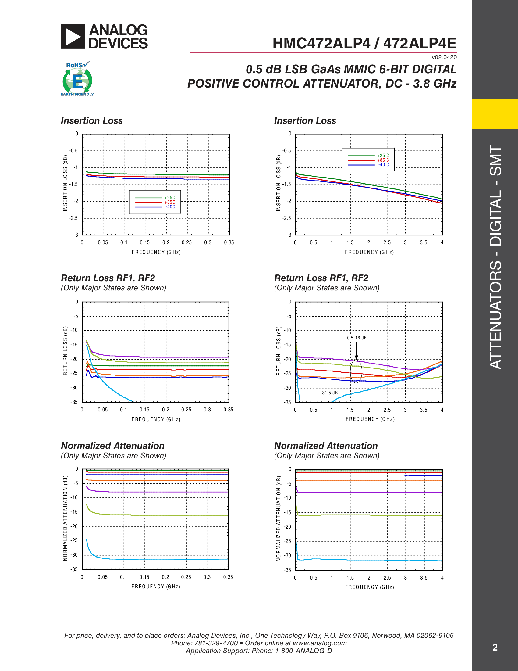
Temperature curves shown for:
- +25°C
- +85°C
- -40°C
Normalized Attenuation vs Frequency
Shows attenuation for major states (0.5-16 dB and 31.5 dB)
Return Loss RF1, RF2 vs Frequency
Return loss performance across 0-4 GHz range
Page 3 - Bit Error Analysis
Bit Error vs. Frequency
Performance curves for different attenuation states:
- 0.5 - 4 dB states
- 8 - 31.5 dB states
Bit Error vs. Attenuation State
Multiple frequency measurements:
- 50 MHz
- 100 MHz, 300 MHz, 350 MHz
- 200 MHz
Bit Error vs. Frequency without AC Ground Caps
Shows behavior when AC ground capacitors are omitted (for reference)
Page 4 - Control Interface
Worst Case Step Error
Between successive attenuation states across frequency range (0-4 GHz)
Relative Phase vs. Frequency
Phase shift for major attenuation states:
- 0.5-4 dB
- 8 dB
- 16 dB
- 31.5 dB
Truth Table
| V1 (16 dB) | V2 (8 dB) | V3 (4 dB) | V4 (2 dB) | V5 (1 dB) | V6 (0.5 dB) | Attenuation State RF1 - RF2 |
|---|---|---|---|---|---|---|
| High | High | High | High | High | High | Reference I.L. |
| High | High | High | High | High | Low | 0.5 dB |
| High | High | High | High | Low | High | 1 dB |
| High | High | High | Low | High | High | 2 dB |
| High | High | Low | High | High | High | 4 dB |
| High | Low | High | High | High | High | 8 dB |
| Low | High | High | High | High | High | 16 dB |
| Low | Low | Low | Low | Low | Low | 31.5 dB |
Note: Any combination of the above states will provide an attenuation approximately equal to the sum of the bits selected.
Control Voltage
| State | Bias Condition |
|---|---|
| Low | 0 to +0.8 Vdc @ -5 µA Typ. |
| High | +2.0 to +5.0 Vdc @ 40 µA Typ. |
Bias Voltage & Current (Vdd = +5V ± 10%)
| Vdd (V) | Idd (Typ.) (mA) |
|---|---|
| +4.5 | 2.4 |
| +5.0 | 2.5 |
| +5.5 | 2.6 |
Page 5 - Absolute Maximum Ratings
| Parameter | Value |
|---|---|
| RF Input Power (DC - 3 GHz) | +28 dBm (T = +85 °C) |
| Control Voltage Range (V1 to V6) | -1V to Vdd +1V |
| Bias Voltage (Vdd) | +7V |
| Channel Temperature | 150 °C |
| Continuous Pdiss (T = 85 °C) | 0.56 W (derate 8.6 mW/°C above 85 °C) |
| Thermal Resistance | 116 °C/W |
| Storage Temperature | -65 to +150 °C |
| Operating Temperature | -40 to +85 °C |
| ESD Sensitivity (HBM) | Class 1A |
⚠️ ELECTROSTATIC SENSITIVE DEVICE - OBSERVE HANDLING PRECAUTIONS
Package Information
| Part Number | Package Body Material | Lead Finish | MSL Rating | Package Marking |
|---|---|---|---|---|
| HMC472ALP4 | Low Stress Injection Molded Plastic | Sn/Pb Solder | MSL3 [1] | H472A XXXX |
| HMC472ALP4TR | Low Stress Injection Molded Plastic | Sn/Pb Solder | MSL3 [1] | H472A XXXX |
| HMC472ALP4E | RoHS-compliant Low Stress Injection Molded Plastic | 100% matte Sn | MSL3 [2] | H472A XXXX |
| HMC472ALP4ETR | RoHS-compliant Low Stress Injection Molded Plastic | 100% matte Sn | MSL3 [2] | H472A XXXX |
[1] Max peak reflow temperature of 235 °C [2] Max peak reflow temperature of 260 °C [3] 4-Digit lot number XXXX
Outline Drawing
24-Lead Lead Frame Chip Scale Package [LFCSP] 4 mm × 4 mm Body and 0.85 mm Package Height (CP-24-16)
Package dimensions (mm):
- Body: 4.00 SQ (3.90-4.10)
- Height: 0.85 (0.80-0.90)
- Lead pitch: 0.50 BSC
- Exposed pad: 2.70 SQ (2.60-2.80)
Page 6 - Pin Descriptions
| Pin Number | Function | Description |
|---|---|---|
| 1, 3, 5, 12, 14, 16, 17, 18 | N/C | These pins should be connected to PCB RF ground to maximize performance. |
| 2 | Vdd | Supply Voltage. |
| 4, 15 | RF1, RF2 | This pin is DC coupled and matched to 50 Ohm. Blocking capacitors are required. Select value based on lowest frequency of operation. |
| 6 - 11, 13 | ACG1 - ACG7 | External capacitors to ground are recommended for low and high frequency operation. Select value for lowest frequency of operation. Place capacitor as close to pins as possible. For operation from 700 to 2700 MHz, these pins may be left unconnected. |
| 19 - 24 | V1 - V6 | See truth table and control voltage table. |
| GND | Exposed Paddle | Package bottom has an exposed metal paddle that must also be connected to RF/DC Ground. |
Page 7 - Application Circuit
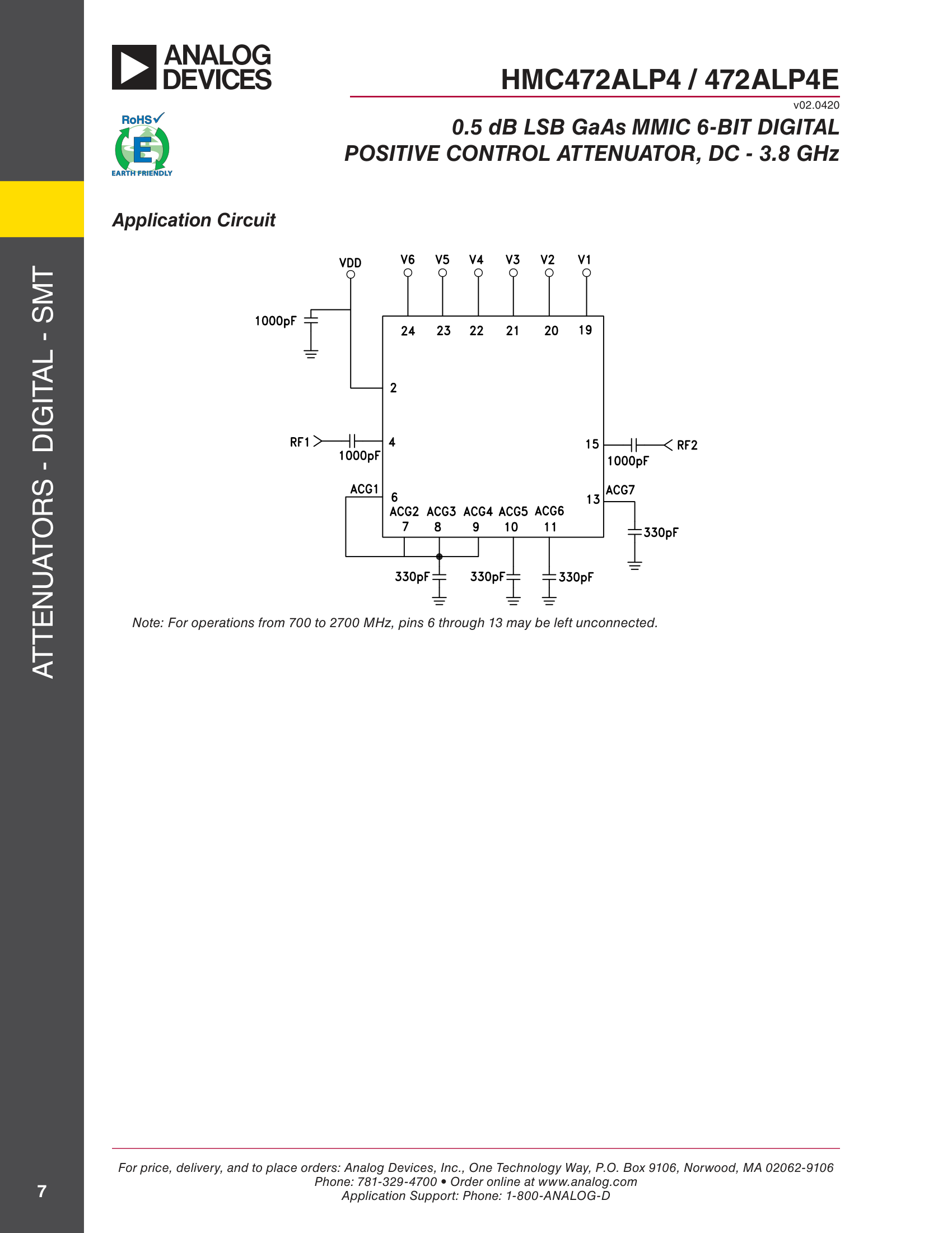
Note: For operations from 700 to 2700 MHz, pins 6 through 13 may be left unconnected.
Page 8 - Evaluation PCB
The circuit board used in the application should use RF circuit design techniques. Signal lines should have 50 Ohm impedance while the package ground leads and exposed paddle should be connected directly to the ground plane similar to that shown. A sufficient number of via holes should be used to connect the top and bottom ground planes. The evaluation circuit board shown is available from Analog Devices, upon request.
List of Materials for Evaluation PCB 107010 - HMC472ALP4 [1]
| Item | Description |
|---|---|
| J1 - J2 | PCB Mount SMA Connector |
| J3 | 14 Pin DC Connector |
| C1 | 1000 pF Capacitor, 0603 Pkg. |
| C2, C3 | 1000 pF Capacitor, 0402 Pkg. |
| C4 - C7 | 330 pF Capacitor, 0402 Pkg. |
| U1 | HMC472ALP4E Digital Attenuator |
| PCB [2] | 106977 Evaluation PCB |
[1] Reference this number when ordering complete evaluation PCB [2] Circuit Board Material: Rogers 4350