Datasheet extraction, module specs, marketing photos, and
project CLAUDE.md with local resource inventory.
5.9 KiB
HMC472A Digital RF Attenuator - Module Specifications
Extracted from Analog Devices HMC472A datasheet for the Amazon module variant.
Electrical Specifications
Test Conditions: T_A = +25°C, Vdd = +5V, Vctl = 0/+5V (unless otherwise noted)
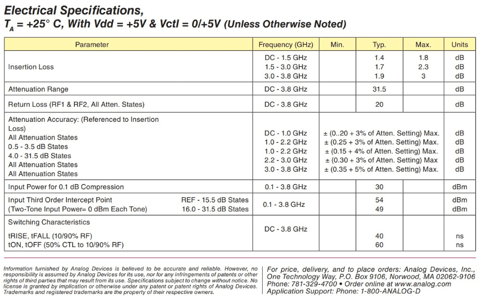
| Parameter | Frequency | Min | Typ | Max | Units |
|---|---|---|---|---|---|
| Insertion Loss | DC - 1.5 GHz | — | 1.4 | 1.8 | dB |
| 1.5 - 3.0 GHz | — | 1.7 | 2.3 | dB | |
| 3.0 - 3.8 GHz | — | 1.9 | 3.0 | dB | |
| Attenuation Range | DC - 3.8 GHz | — | 31.5 | — | dB |
| Return Loss (RF1 & RF2, All States) | DC - 3.8 GHz | — | 20 | — | dB |
Attenuation Accuracy
Referenced to insertion loss:
| Attenuation States | Frequency | Max Error |
|---|---|---|
| All States | DC - 1.0 GHz | ±(0.20 + 3% of Setting) dB |
| 0.5 - 3.5 dB States | 1.0 - 2.2 GHz | ±(0.15 + 4% of Setting) dB |
| 4.0 - 31.5 dB States | 2.2 - 3.0 GHz | ±(0.30 + 3% of Setting) dB |
| All States | 3.0 - 3.8 GHz | ±(0.35 + 5% of Setting) dB |
Power Handling & Linearity
| Parameter | Frequency | Value | Units |
|---|---|---|---|
| Input Power for 0.1 dB Compression | 0.1 - 3.8 GHz | 30 | dBm |
| IIP3 (Two-Tone, 0 dBm each) | |||
| — REF to 15.5 dB States | 0.1 - 3.8 GHz | 54 | dBm |
| — 16.0 to 31.5 dB States | 0.1 - 3.8 GHz | 49 | dBm |
Switching Characteristics
| Parameter | Frequency | Typical | Units |
|---|---|---|---|
| t_RISE, t_FALL (10/90% RF) | DC - 3.8 GHz | 40 | ns |
| t_ON, t_OFF (50% CTL to 10/90% RF) | DC - 3.8 GHz | 60 | ns |
Bias Voltage & Current
Supply: Vdd = +5V ± 10%
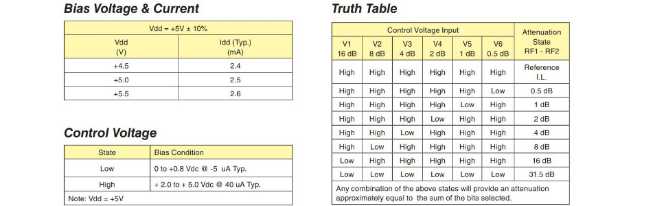
| Vdd (V) | Idd Typical (mA) |
|---|---|
| +4.5 | 2.4 |
| +5.0 | 2.5 |
| +5.5 | 2.6 |
Control Voltage States
| State | Bias Condition |
|---|---|
| Low | 0 to +0.8 Vdc @ -5 µA Typ. |
| High | +2.0 to +5.0 Vdc @ 40 µA Typ. |
Note: Vdd = +5V
Truth Table
Each control pin (V1-V6) contributes a specific attenuation value when set Low:
| Pin | Attenuation Value |
|---|---|
| V1 | 16 dB |
| V2 | 8 dB |
| V3 | 4 dB |
| V4 | 2 dB |
| V5 | 1 dB |
| V6 | 0.5 dB |
Example Attenuation States
| V1 (16dB) | V2 (8dB) | V3 (4dB) | V4 (2dB) | V5 (1dB) | V6 (0.5dB) | Total Attenuation |
|---|---|---|---|---|---|---|
| High | High | High | High | High | High | Reference (I.L.) |
| High | High | High | High | High | Low | 0.5 dB |
| High | High | High | High | Low | High | 1 dB |
| High | High | High | Low | High | High | 2 dB |
| High | High | Low | High | High | High | 4 dB |
| High | Low | High | High | High | High | 8 dB |
| Low | High | High | High | High | High | 16 dB |
| Low | Low | Low | Low | Low | Low | 31.5 dB |
Note: Any combination of the above states will provide an attenuation approximately equal to the sum of the bits selected.
Functional Diagram & Pinout
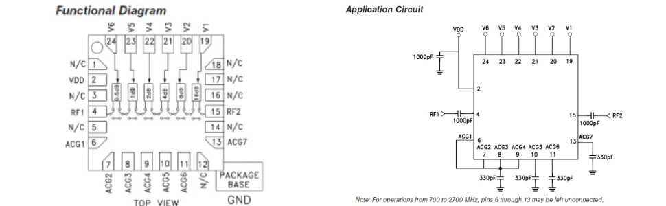
Pin Assignment (24-Pin QFN, Top View)
| Pin | Function | Pin | Function |
|---|---|---|---|
| 1 | N/C | 13 | ACG7 |
| 2 | VDD | 14 | N/C |
| 3 | N/C | 15 | RF2 |
| 4 | RF1 | 16 | N/C |
| 5 | N/C | 17 | N/C |
| 6 | ACG1 | 18 | N/C |
| 7 | ACG2 | 19 | V1 (16 dB) |
| 8 | ACG3 | 20 | V2 (8 dB) |
| 9 | ACG4 | 21 | V3 (4 dB) |
| 10 | ACG5 | 22 | V4 (2 dB) |
| 11 | ACG6 | 23 | V5 (1 dB) |
| 12 | N/C | 24 | V6 (0.5 dB) |
| Base | GND |
Application Circuit
Recommended Component Values
| Reference | Value | Function |
|---|---|---|
| C1 | 1000 pF | VDD bypass capacitor |
| C2 | 1000 pF | RF1 DC blocking / coupling |
| C3 | 1000 pF | RF2 DC blocking / coupling |
| C4-C8 | 330 pF | ACG2-ACG6 bypass capacitors |
| C9 | 330 pF | ACG7 bypass capacitor |
Circuit Notes
- VDD (pin 2) requires 1000 pF bypass to ground
- RF1 (pin 4) and RF2 (pin 15) use 1000 pF DC blocking capacitors for AC coupling
- ACG pins (ACG2-ACG6 on pins 7-11, ACG7 on pin 13) require 330 pF bypass capacitors to ground
Note: For operations from 700 MHz to 2700 MHz, pins 6 through 13 (ACG1-ACG7) may be left unconnected.
Performance Graphs
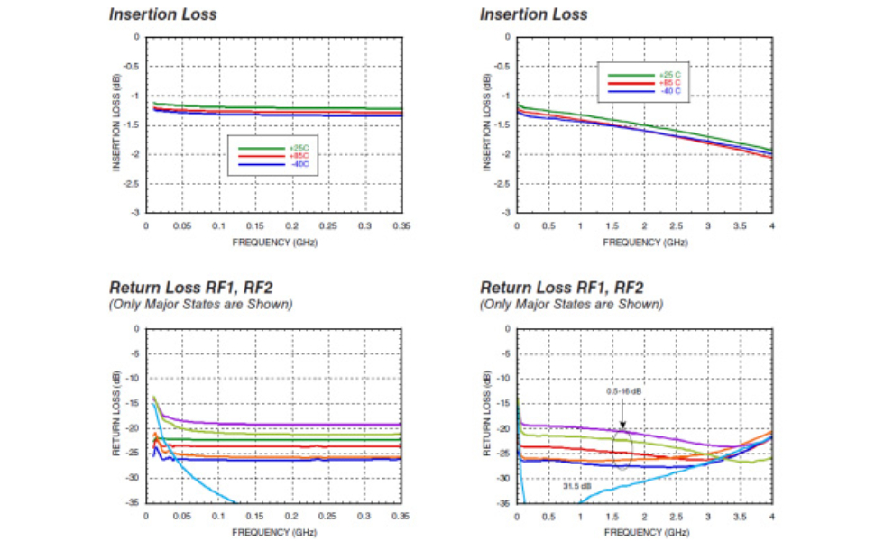
Insertion Loss vs Frequency
Two graphs showing insertion loss across temperature (+25°C, +85°C, -40°C):
-
Low Frequency Range (DC - 350 MHz)
- Insertion loss approximately 1.0 to 1.2 dB
- Minimal temperature variation
-
Full Frequency Range (DC - 4 GHz)
- Insertion loss increases from ~1.2 dB at low frequencies to ~2.0 dB at 4 GHz
- Temperature variation more pronounced at higher frequencies
- -40°C shows best performance, +85°C shows highest loss
Return Loss RF1 & RF2
Two graphs showing return loss for major attenuation states:
-
Low Frequency Range (DC - 350 MHz)
- Return loss typically better than -15 dB across all states
- Best performance around 100 MHz
-
Full Frequency Range (DC - 4 GHz)
- Reference and low attenuation states (0.5-16 dB): -15 to -25 dB return loss
- Maximum attenuation state (31.5 dB): return loss degrades above 2 GHz
- All states maintain better than -10 dB return loss across band
Quick Reference Summary
| Specification | Value |
|---|---|
| Frequency Range | DC - 3.8 GHz |
| Attenuation Range | 0 - 31.5 dB |
| Step Size | 0.5 dB |
| Insertion Loss (typ) | 1.4 - 1.9 dB |
| Return Loss (typ) | 20 dB |
| IIP3 | 49 - 54 dBm |
| Supply Voltage | +5V ± 10% |
| Supply Current | 2.5 mA typ |
| Switching Speed | 40 - 60 ns |
| Package | 24-pin QFN |
| Input/Output Impedance | 50Ω |